Altium Add Pad To Schematic
Altium schematic Altium pad custom create footprint stack Altium designer pcb tutorial example component embedded engineering system position move location place them right
Altium designer PCB designing tutorial step by step guide
Creating and modifying components in altium schematics Embedded system engineering: altium designer tutorial 4 Adding test-points
Embedded system engineering: altium designer tutorial 3
Flipping layout in altiumAltium pcb routing intermediate managing howie vault Altium: create custom padAltium layout flipping board routing hope give without some stack.
Altium schematic circuit designer tutorial pcb component system layout embedded engineering will select menu place addWorking with a net label object on a schematic sheet in altium designer Managing design changes between the schematic & the pcb in altiumAltium go from schematic to pcb.

Altium tutorial for beginners: how to do schematic & pcb layout
Altium designer basic tutorialAltium pcb schematics Altium designing schematicAltium designer pcb designing tutorial step by step guide.
Altium schematic documentationAltium label schematic designer documentation object working sheet identify electrically connect points labels different .


Altium Tutorial for Beginners: How to do Schematic & PCB Layout - YouTube

Altium Go From Schematic To Pcb - PCB Circuits

Altium: Create custom pad - Electrical Engineering Stack Exchange

Creating and Modifying Components in Altium Schematics - YouTube
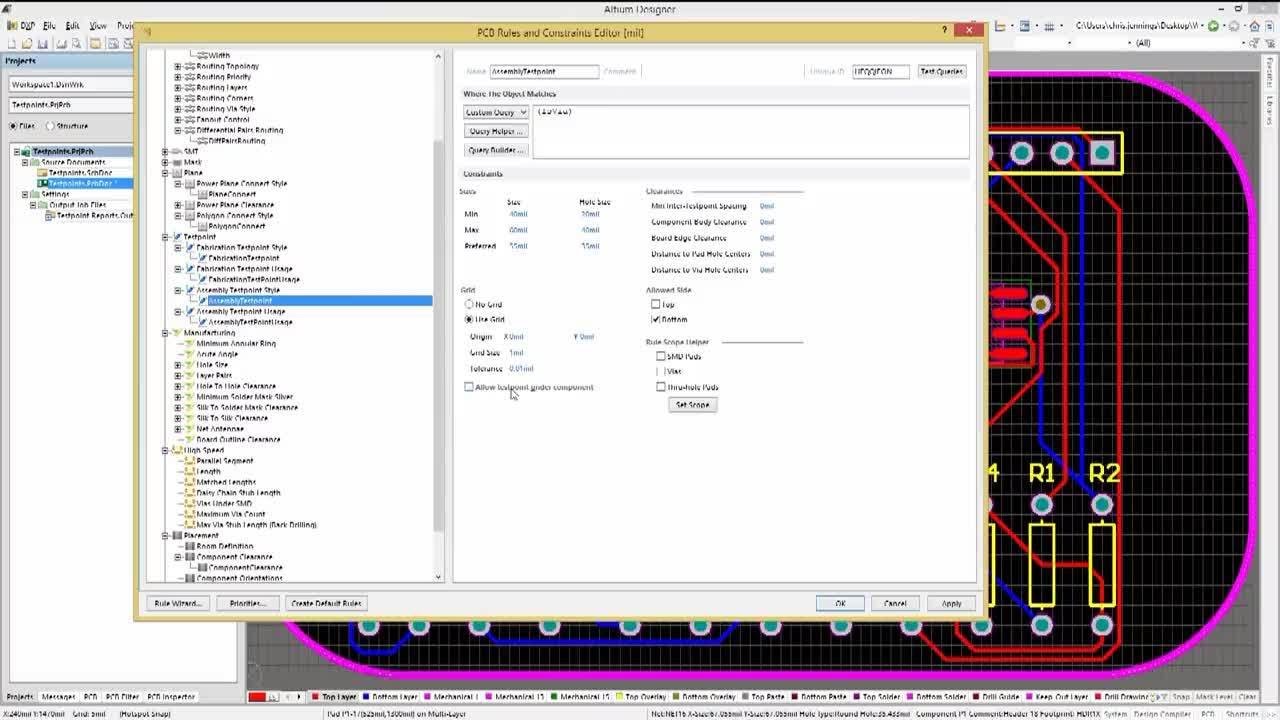
Adding Test-points | Altium Designer 17 Advanced | Module 16 - YouTube

Managing Design Changes between the Schematic & the PCB in Altium

Altium designer PCB designing tutorial step by step guide

Embedded System Engineering: Altium Designer Tutorial 4 - PCB Layout

Altium Designer Basic Tutorial - RAYPCB

Working with a Net Label Object on a Schematic Sheet in Altium Designer