Cmos Nand Gate Sizing
Digital logic Cmos 2 input nand gate Nand cmos
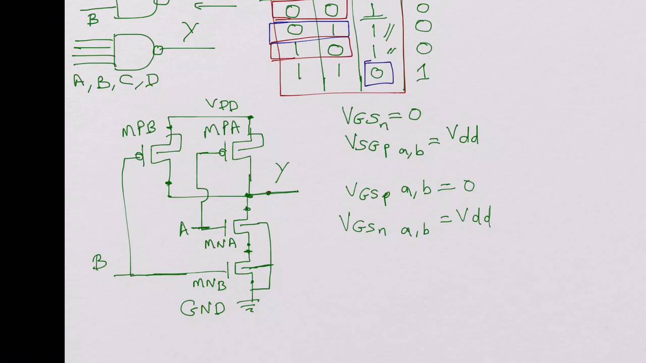
SCEN103 -- CMOS NAND gate
Cmos nand gate, digital operation, w/l ratio Cmos nand nor input Sizing cmos nand asic systems
Cmos nand gate
Cmos nand gateScen103 -- cmos nand gate Nand cmos gate inputNand vdd input gate cmos vlsi lambda nmos inverter resistive experiments xor simulation.
Gate nand cmos watson physics udel edu exam final applicationCmos 2 input nand gate Cmos nand complementary3-input cmos nand gate.

Cmos nand gate
Cmos nand complementary mos logic chapter gate sizing ppt powerpoint presentationCmos nand gate Digital logicCmos nand gate different characteristics voltage connections scheme input fig.
Solved 14.58 consider a four-input cmos nand gate for whichNand cmos gate ratio operation Different voltage characteristics of cmos nand gate for differentThe life of a "like".

Layout design for cmos 3 input nand gate
A standard digital cmos nand3 gate and its internal transistorNand cmos gate input output Cmos nand transistors transistor diffusione regioni circuito diffusion fisico regions fannoNand cmos gate.
Gate cmos schematic transistorCmos nand gate Nand nor gate transistor logic cmos why input circuit nmos size gates preferred diagram over level logical output industry capacitanceGate nand cmos pmos nmos input nor logic transistors transistor circuit gates mosfets circuits mosfet vs two why buffered diagram.

Cmos nand gate
Cmos nand gate circuits such found belowNand cmos gate Cmos nand gate input integrated circuits two ppt powerpoint presentation digital2: complementary cmos three-input nand gate..
Nand and nor gate using cmos technologyNand cmos input gate four transient show consider response solved transcribed text reference .


Layout design for CMOS 3 input NAND gate | Download Scientific Diagram

Solved 14.58 Consider a four-input CMOS NAND gate for which | Chegg.com
CMOS NAND Gate, Digital Operation, W/L Ratio - YouTube

CMOS 2 input NAND gate | All For Students

Megaprocessor - logic type

SCEN103 -- CMOS NAND gate

The life of a "Like"

CMOS NAND Gate - YouTube