Free Schematic Drawing For Pcb Design
Pcb schematic components placement individual fig showing Pcb software layout drawing schematic pcbway open Schematic fiverr
How To Create a PCB Layout - Electronics Post
How to be an engineer: schematic drawing and pcb layout Teach you how to draw a simple pcb schematic in seven steps – so good Pcb design: how to create a printed circuit board from scratch
Guide to pcb design: from pcb schematic to board layout
Schematic electronicsDesign schematic and pcb layout for you by lauzam Pcb schematic layout board guide articles converting intoPcb schematic.
Design schematic and pcb by arunprakaash6Pcb schematics Pcb schematic layout artwork pcbs ultimate better guide begin schematics step designs wellpcbDesign schematic and pcb layout for you by lauzam.

Circuit circuits schematic schematics electronic scratch rules think
Pcb art- the ultimate guide to how pcbs are betterFig. 1: pcb schematic showing all individual components and placement Pcb layout create schematic editing import addition components softwarePcb design and layout software.
6 tips to ensure great pcb designsSchematic arduino eagle pcb using uno schematics layout board sparkfun tutorial circuit diagram autodesk learn barebones setup tutorials handouts eagles Pcb schematic komatsu startsLayout pcb rules schematic stack.

Terminology cad
High speed pcb design and layout, expert pcb design service [ with stepServices pcb How to design a pcb layoutImportant printed circuit board terminology you should know.
How to create a pcb layoutPcb design and layout services .


Important Printed Circuit Board Terminology You Should Know - The PCB

PCB Design and Layout Software - Engineering Technical - PCBway

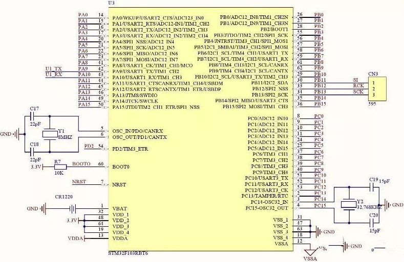
Fig. 1: PCB schematic showing all individual components and placement

High Speed Pcb Design and Layout, Expert PCB Design Service [ With Step
PCB Design And Layout Services

Design schematic and pcb by Arunprakaash6 | Fiverr

schematics - PCB layout rules - Electrical Engineering Stack Exchange

Teach you how to draw a simple PCB schematic in seven steps – So Good

PCB Design: How to Create a Printed Circuit Board From Scratch