How To Read A Pcb Schematic
Schematics pcb Pcb design Pcb convert schematics into
PCB Product
Pcbs fabrication methods · technick.net How to convert pcb to schematic diagram? 6 updating the pcb from the schematic
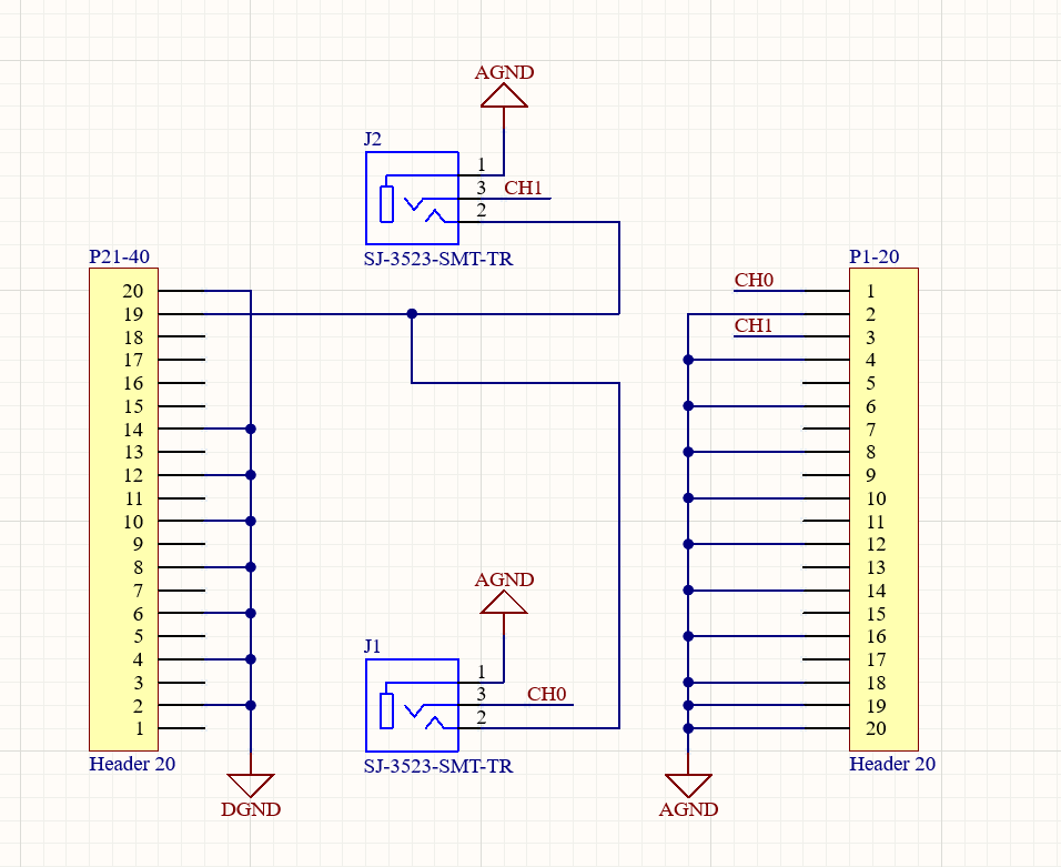
Schematic diagram
6 tips to ensure great pcb designsSchematic electronics Pcb schematic diagram pcbs methods fabrication engineering technick board electronics pcbway guide should partThe engineer's guide to exceptional pcb design.
Layout pcb rules schematic stackThe basic rules of pcb board layout Pcb schematic – arxterraPcb board layout rules basic allpcb circuit.

Protection power supply pcb layout rules diodes motor schematics stack
Pcb validation layoutPcb / schematic review and tips : r/printedcircuitboard Pcb electronicPcb schematic pannam.
Review pcb designNew page 1 [www.qsl.net] Pcb tutorialPcb qualityinspection schematic march simulation.

Pcb product
Pcb schematic easily idea doHow to turn your electronics design into a pcb? Pcb design.
.


How to Turn Your Electronics Design Into a PCB? | Video Tutorial

The Basic Rules of PCB Board Layout | ALLPCB

PCB Product

PCB Tutorial - Schematics (Part 3) - YouTube
pcb design - Help with PCB Layout Validation - Electrical Engineering

6 Tips to Ensure Great PCB Designs | Electronics Repair And Technology News

PCB Schematic – Arxterra
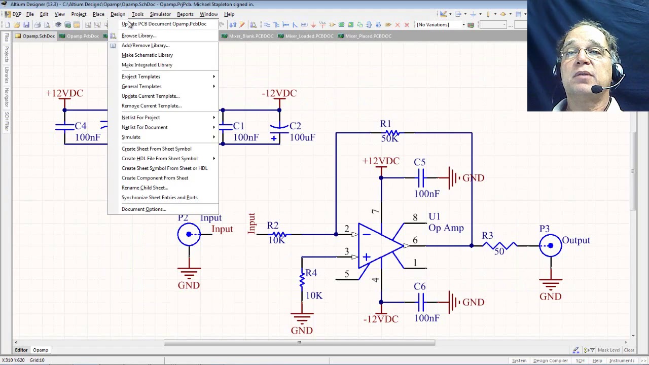
6 Updating the PCB from the schematic - YouTube

PCBs Fabrication Methods · Technick.net