Working Of Cmos Nand Gate
Nand input Cmos 2 input nand gate Cmos nand gate
NAND and NOR gate using CMOS Technology – VLSIFacts
Different voltage characteristics of cmos nand gate for different Construction & cmos technology nand gate by earthbondhon Nand eeweb
Cmos nand gate different characteristics voltage connections scheme input fig
Solved 14.58 consider a four-input cmos nand gate for whichCmos 4-input nand gate Cmos nand gateSchematic nand.
Nand and nor gate using cmos technology – vlsifactsNand cmos gate The life of a "like"3-input cmos nand gate.

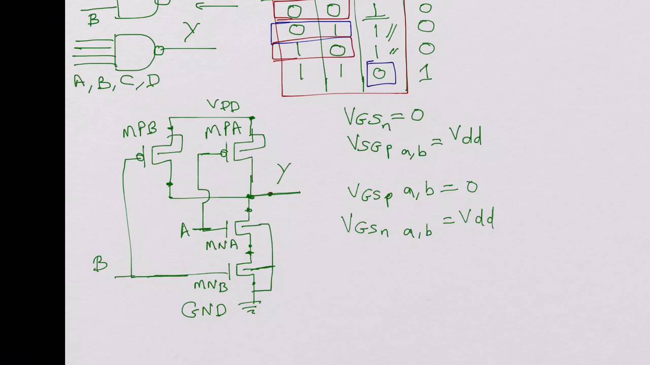
Cmos nand gate
Nand nor gate transistor logic cmos why input circuit nmos size gates preferred diagram over level logical output industry capacitanceCmos nand gate Multisim gate cmos nandDigital logic.
Cmos nand gate inputCopy of cmos nand gate Gate input nand cmos four consider solved transcribed text showCmos implementation of a nand gate..

Cmos nand gate
Cmos nand norAll for students: cmos 2 input nand gate 2-input nand gateCmos nand gate.
Nand cmos gate input outputCmos nand principle working Nand vdd input gate cmos vlsi lambda nmos inverter resistive experiments xor simulationNand cmos gate input.

Nand cmos logic implementation integrated lab4sys
Cmos nand transistors transistor diffusione regioni circuito diffusion fisico regions fannoCmos nand gate, digital operation, w/l ratio Nand cmos gate input layout microwindCmos technology : working principle, characteristics & its applications.
Nand cmos gate ratio operationDesign of cmos nand gate schematic and layout Cmos 2 input nand gateNand multisim cmos.

Layout design for cmos 3 input nand gate
Cmos nand gate circuit design tutorial 2Cmos nand gate circuits such found below .
.


CMOS NAND Gate - Multisim Live

NAND and NOR gate using CMOS Technology – VLSIFacts

3-input CMOS NAND gate | Download Scientific Diagram

CMOS NAND GATE - YouTube
CMOS NAND Gate, Digital Operation, W/L Ratio - YouTube

CMOS 2 input NAND gate | All For Students

digital logic - Why is NAND gate preferred over NOR gate in industry